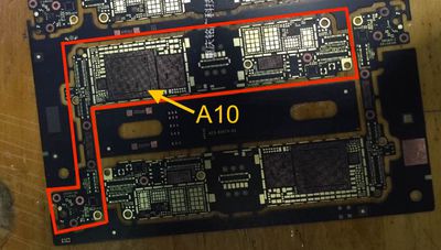
![]() Last year, MacRumors covered the potential reasoning for Apple's rumored return to having a single partner for Apple A-series chip production with the A10 after having both Samsung and TSMC produce versions of the Apple A9.
Last year, MacRumors covered the potential reasoning for Apple's rumored return to having a single partner for Apple A-series chip production with the A10 after having both Samsung and TSMC produce versions of the Apple A9.
Since then, TSMC confirmed in conference call comments that its chip packaging changes have led to improvements of 20 percent in both speed and packaging thickness and 10 percent in thermal performance. This has a number of implications for future device performance and future foundry partner selection for Apple.
First, it is helpful to understand why InFO-WLP (Integrated Fan-Out Wafer-Level Packing) is such an important development for Apple's mobile processors. Typically, chips as large as CPUs or mobile SoCs have been attached via "flip-chip" methods which attach an array of inputs and outputs to a package substrate via solder bumps, ultimately enabling it to be attached to a printed circuit board (PCB) for device integration.
From the start, this is a compromise, as it would be preferable to attach a silicon die directly to the PCB to minimize height and reduce the lengths of interconnects between components. A number of technical limits in areas such as interconnect pitch, board produceability, and damage due to board warpage typically prevent this direct attachment.
The above problem had previously been circumvented for smaller I/O count components with a similar concept called Fan-In Wafer-Level Packing, where smaller dies are allowed to route their inputs and outputs in an area roughly the same area as the die. TSMC is just one of many companies beginning to enable this concept for larger I/O count devices in such a way that allows high volume, acceptable yields, and an acceptable cost.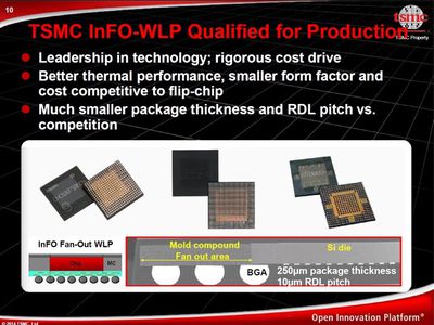
With this method, the traditional substrate becomes unnecessary, as a silicon wafer serves that purpose with one or more logic dies included. The reduced height of this method and a thinner redistribution layer (RDL) for remapping pins of the die to the PCB means that all interconnects are shorter, which directly enables lower power and better thermal performance. The transistors driving the outputs on this device now drive less metal length, meaning they can save power. Saving power also means performing better thermally, but a more direct connection to the PCB means there is simply less thermal resistance to the PCB, which can pull heat away from the device.
The promised performance improvements are certainly significant. A 20 percent improvement in performance is roughly equivalent to the improvement expected between successive foundry nodes (e.g. the change from 14 nm to 10 nm). With both TSMC and Samsung only offering refined versions of their 16 nm and 14 nm FinFET processes, this means that total performance gains could be in line with the same improvement seen from the A8 to the A9 chip, but driven by packaging improvements rather than a new process.
Of course, every generation can't enjoy this same improvement, but increased power efficiency is critical for mobile devices to be allowed to hit higher peak limits for short durations. In the keynote for the iPhone 6 family of devices, Apple went into detail about how it made a significant effort to ensure the A8 processor did not throttle itself as the A7 had. This was and is an industry-wide problem as mobile SoC makers have raced to provide the highest performing chips. By taking advantage of new packaging from TSMC, Apple gets more relief in this metric, and freedom to go to a higher power dissipation mode for short periods.
A long-term advantage of this technology is to enable much faster main memory interfaces to the logic die, largely by widening the interface. Current mobile SoC packages use PoP (package-on-package) techniques which connect the memory dies to the main processor with tiny wires, which is thermally inefficient and not ideal for performance. By using wafer-level packaging, these drawbacks can be reduced for the main memory, while also increasing the number of connections and data that can be moved in a given time.
In the long run, this move will likely be a cost-saver for Apple as it removes the package substrate. However, the co-design of device die and device package explains why multiple partners are not technically feasible for an effort such as this. Companies like TSMC have also labored for years to make this a reality, with the benefits long being understood.
At this point, there is no denying Apple's technical acumen and bandwidth in chip design. The company has developed multiple chips for market in extremely aggressive timeframes with fully custom designs that rival those of Intel for performance per watt. Apple beat its competitors to market for a 64-bit ARM design by over a year, and designed two custom A9 dies in the time that its competitors designed one.
Given Apple's focus on pushing the performance of its silicon, and TSMC's packaging advancements, it makes sense that TSMC has been able to gain sole possession of Apple's chip orders for at least this generation. Looking forward, the InFO-WLP packaging technique marks a significant development not only for TSMC and Apple, but the semiconductor industry as a whole.